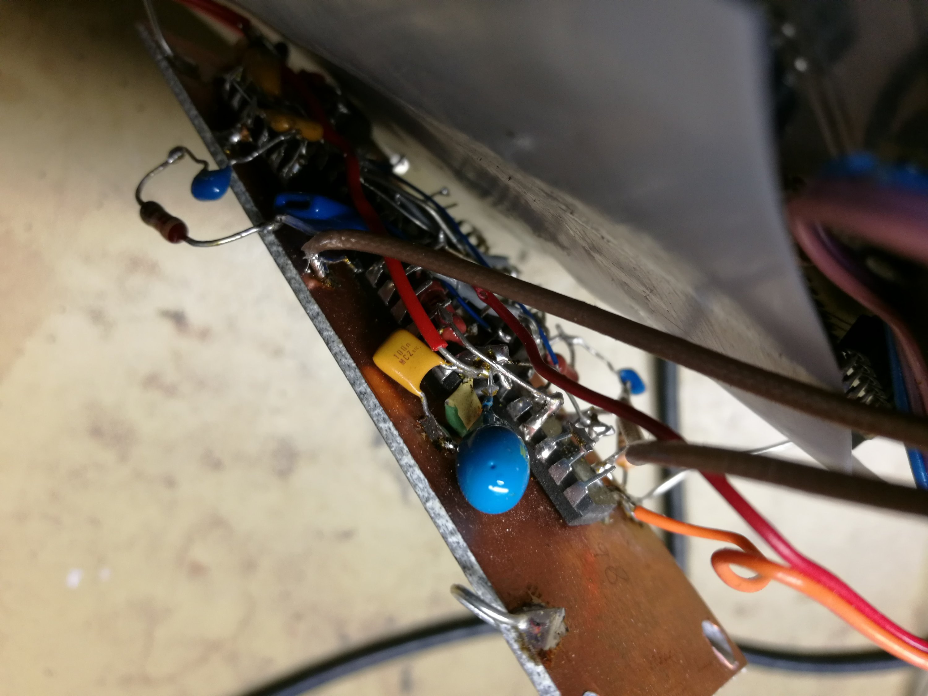
Dead bug prototyping
“Dead bug style” circuit wiring is the cute name for soldering together components without a printed circuit board. The “dead bug” is the integrated circuit flipped upside down with its “legs” sticking up. The chips can be glued to almost any surface, but most often the surface material is circuit board with copper (the copper is usually used as ground plane in circuit). Dead-bug construction is very straightforward and requires no special tools.
Dead bug construction is one form of Free-form construction suitable for a small number of components.In “dead bug” style the ICs flipped upside-down with their pins sticking up into the air like a dead insect. This form of construction is used by amateurs for one-off circuits for circuits with few components. Dead-bug construction generally becomes impractical once the IC pin count exceeds 20 pins or if there are more than two or three ICs.
This construction is often used for RF circuits where component leads must be kept short. For high-frequency work a grounded solderable metallic base such as the copper side of an unetched printed circuit board can be used as base and ground plane.To make the connections, components are mostly soldered directly together, lead to lead. The dead-bug style helps to eliminate capacitive coupling between traces by building the traces in the air to maximize the distance and minimize the parallel runs that various leads travel with one another.
Linear Technology application note 47 gives introduction to this construction method for quite high frequency. Dead Bug Prototyping for Effects shows how to build audio circuits. The following video shows how to do dead bug with SMD components:

2 Comments
Hanna says:
Great video geometry dash online. I watched it.
annakenna says:
“Dead bug style” circuit wiring, also known as rice purity test, involves soldering components without a printed circuit board. This method is straightforward and requires no special tools, making it suitable for a small number of components. However, it becomes impractical for circuits with more than 20 pins or multiple ICs. This construction technique is often used in high-frequency applications to eliminate capacitive coupling between traces.